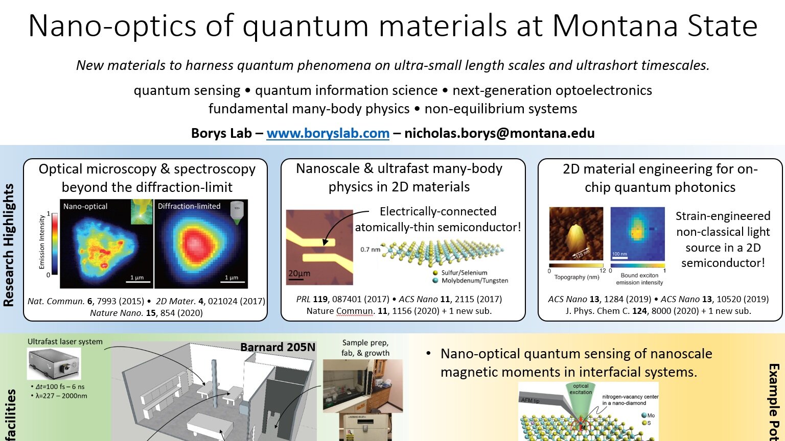
Virtual Lab Tour and Overview
Lab tour video
(warning: we are physicists, not filmmakers!)
Quantum optoelectronics in 2D materials
2D layered materials are naturally occurring and synthetic systems that are composed of sheets of atoms that are only a few atomic layers thick in one dimension and extended in the other two dimensions. Such layered materials can form semiconductors, insulators, superconductors, metals, and other exotic quantum systems such as topological insulators. Several research activities in the Borys Lab focus on using optical spectroscopy to explore, discover, and manipulate the optical and electronic properties of 2D layered materials. By understanding the intricate details behind how 2D materials absorb and emit light, we gain deep insight into their underlying quantum mechanical optical and electronic behavior. Furthermore, with specialized nano-optical and time-resolved optical imaging and spectroscopy tools, we study quantum phenomena in 2D materials on time scales as small as a picosecond (10^-12 s) and at length scales as small as 10 nm (10^-8 m). At these extremes of time and space, we can often discover hidden effects that are missed with other more conventional and less sophisticated techniques, leading to new routes to utilize these materials in technologies ranging from high-performance solar cells and sensors to next-generation applications in quantum information science.

Figure - 2D semiconductors. (a) Schematic of a single layer of transition metal dichalcogenide semiconductors. (b) An image of individual crystallites of single layers of MoS2 taken with a conventional bright field optical microscope. (c) Typical optical absorption and emission spectra of a single layer of MoS2. (d) and (e) a comparison between imaging the light emission from a single crystallite of MoS2 using specialized nano-optical techniques (d) to less-sophisticated diffraction-limited techniques (e).
A schematic of a 2D semiconductor is shown to the left. These systems are composed of a sheet of transition metal atoms (e.g. Mo or W) that are sandwiched between two sheets of chalcogen atoms (e.g. S or Se). A single sheet of these atoms is a fully functional semiconductor (like the Si in your phone) and exhibits remarkably strong light-matter interactions, absorbing about 10% of incident visible light and emitting light at high efficiency (unlike the Si in your phone!). Additionally, because these materials are atomically thin and have unique crystalline symmetry, they also possess a suite of interesting quantum mechanical properties that directly interface to their strong optical properties, making them a great platform to use optical techniques to probe and manipulate quantum phenomena in a solid-state system. From new ways to build a light source that can produce a single photon at a time, to new materials from which to construct qubits, 2D semiconductors have a lot of potential to be important material systems for the next quantum revolution because of this fantastic convergence of properties. Alongside a deep curiosity and love for quantum phenomena, this potential for applications is a significant driver for our research in 2D semiconductors and other 2D quantum materials.
Nanoscale imaging and spectroscopy of quantum materials
There is substantial motivation from a technological standpoint to figure out new ways of harnessing quantum mechanical phenomena in solid-state materials. In comparison to cold atom systems or individual photons, solid-state quantum materials are easier to scale-up and deploy in industrial settings. Additionally, the complex behavior of the large number of electrons in solid-state materials gives rise to new types of quantum phenomena that can be possibly exploited for future technologies. For these reasons, solid-state quantum materials lie at the frontier of many different areas of quantum science.

Figure - Nano-optical imaging & spectroscopy. (a) Schematic of a sharp silver nano-optical antenna probing nanoscale light-matter interactions of quantum emitter states in a nanobubble of monolayer WSe2. (b) Closeup photograph of nano-optical microscopy configuration comprised of a scanning probe head next to a side-illuminating microscope objective with broadband LEDs providing a wide-area light source for imaging.
A lot of quantum phenomena in solid-state materials either occur or are greatly influenced by material properties at ultra-small length scales (i.e., on the nanoscale which is approximately 1000x smaller than the diameter of a human hair). It is therefore important that quantum materials researchers have new tools and techniques to study quantum phenomena at such critical length scales. Traditionally, these length scales are difficult to study with optical techniques that are otherwise powerful characterization techniques for quantum materials. In the Borys Group, we develop new nano-optical based techniques to study quantum phenomena at ultra-small length scales via observing light-matter interactions on the nanoscale. As shown in the figure to the right, the essence of nano-optical techniques is to bring a sharp metal antenna in close proximity to the sample. The antenna then acts to focus light to regions over 20x smaller than what can be achieved in a conventional microscope. We build on this fundamental concept to develop new methods to study the nanoscale optical, electronic, and eventually magnetic properties of quantum materials. The goal of this research is to build new characterization tools for quantum materials and by doing so, uncover unexpected relationships between material structure and composition that drive solid-state quantum (and optoelectronic) functionalities.
Microscope development and automation

Figure - Microscope development and automation collage. (a) Close-up of our customized cryogenic confocal microscope system. (b) Custom Arduino-based rotation stage to control optical excitation density in the cryogenic microscope. (c) A sample of our customized Python code to control our microscopy tools using the ScopeFoundry platform.
For many of the experimental tasks that we undertake in the Borys Lab, we often need to develop new microscopy techniques and capabilities. Our lab consists of several sophisticated and highly customizable microscopy tools (stages, lasers, detectors, electronics, etc.) that enable a rich suite of optical spectroscopy techniques. To get all of these systems working in our microscopes, we often need to develop customized electronics, mounts, and software. Therefore, in addition to our exciting research on nano-optics and quantum materials, we often write our own automation software in Python, develop our own hardware using Arduinos and other simple controllers, and build our own mounts using 3D printers. Much of this is made available to the public for use by other groups through the ScopeFoundry platform. We pride ourselves on being able to perform the necessary development and customization to perform complex spectroscopy and imaging techniques that other research groups find too cumbersome or challenging to take on. These efforts are truly team-oriented and the technology created by one group member typically ends up being a common tool for everyone else in the group.